Technology Pathfinding
Evaluated 200+ publications to identify technology directions and guide polymer hybrid bonding process development.
SEMICONDUCTOR R&D · ADVANCED PACKAGING
Advanced Packaging · Hybrid Bonding · Process Integration · Electronic Materials
Connecting materials, processes, structures and performance to develop reliable next-generation semiconductor packaging technologies.
01 · PROFILE
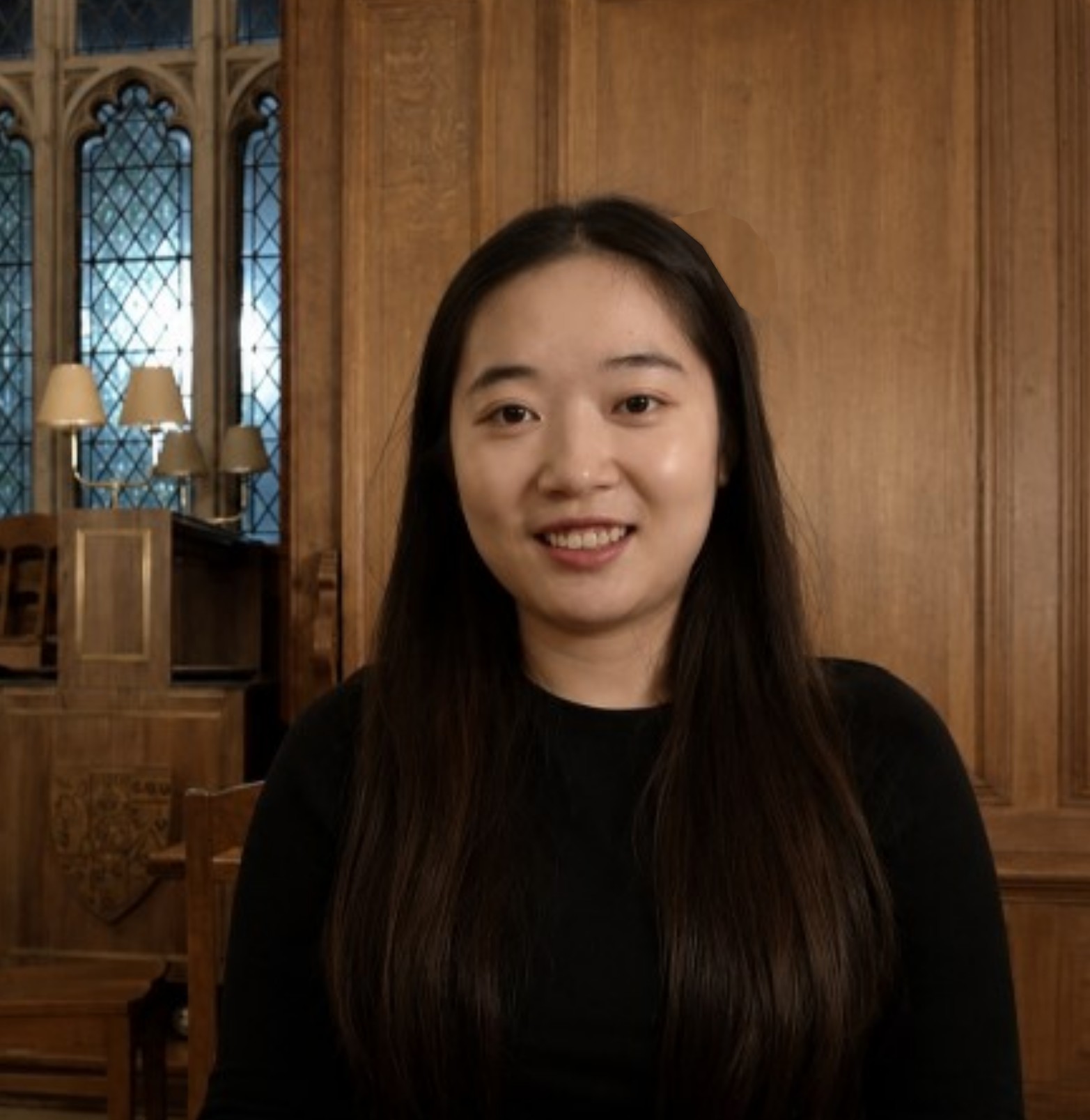
Materials Science PhD from Imperial College London and R&D Senior Engineer at STATS ChipPAC, with experience in advanced packaging, polymer hybrid bonding and process development.
Strong background in process integration, design of experiments, materials characterization and failure analysis, with expertise in understanding material–process–structure–performance relationships for process optimization and reliability improvement.
02 · PROFESSIONAL EXPERIENCE
R&D Senior Engineer · Singapore
TECHNOLOGY DEVELOPMENT
Leading technology development spanning pathfinding, test vehicle design, DOE, process integration, simulation and cross-functional technology alignment.
Evaluated 200+ publications to identify technology directions and guide polymer hybrid bonding process development.
Designed daisy-chain and four-point test vehicles, defined process flows and structures, and developed DOE plans for process-window development and optimization.
Developed hybrid bonding process flows involving lithography, PVD, Cu electroplating, CMP, plasma treatment, dicing and TCB.
Performed ANSYS-based thermo-mechanical simulations to evaluate structural integrity and screen process and design solutions.
Worked with internal teams, research institutes, material suppliers and equipment vendors on simulation, material evaluation, process development and technology alignment.
Root-cause analysis of packaging material and interface defects to support process optimization, yield improvement and reliability enhancement.
Automated detection and quantification of pin offset, saw street quality and die offset from thousands of OM images, reducing manual analysis time by 99%.
Applied JMP for SPC, Cpk and yield analysis, together with Monte Carlo simulation for process-variation assessment.
Developed and standardized contact-angle and shear-strength measurement methods and work instructions.
Built a Python-based data-analysis and reporting workflow, reducing processing time from hours to seconds.
03 · PHD RESEARCH · ELECTRONIC MATERIALS & INTERCONNECTS
PhD Researcher · Oct 2020 — Feb 2025 · Imperial Research Profile ↗
Supervisor
Prof. Christopher M. Gourlay
Research on low-temperature solder materials for electronic packaging, with emphasis on solidification, microstructure evolution, crystallography, interface reactions and solder-joint reliability.
1,000+ hours of hands-on SEM, EBSD and EDX experience.
Investigated Sn–Bi and In–Sn–Bi solder alloys, linking processing conditions with microstructure evolution and performance.
Applied in-situ high-temperature EBSD, time-lapse SEM, TEM diffraction and MATLAB-based MTEX.
Collaborated with Tokamak Energy on ultra-low-temperature In–Sn–Bi solder materials for prototype applications.
04 · PUBLICATIONS, AWARDS & CONFERENCES
IEEE Electronics Packaging Technology Conference (EPTC) · Abstract accepted
Journal of Alloys and Compounds · Vol. 1035 · 181339
DOI ↗Materialia · Vol. 43 · 102524
DOI ↗Acta Materialia · Vol. 189 · 85–92
DOI ↗Awarded for research on Sn-Bi low-temperature solders; selected for presentation at the TMS 2027 Annual Meeting.
Acta Student Award Recipients ↗05 · PATENTS & INNOVATION
U.S. Patent Application Filed
U.S. Patent Application Filed
U.S. Patent Application Filed
06 · TECHNICAL SKILLS
SEM (BSE, EDX) · EBSD · FIB · TEM diffraction · DSC · OM
Python · JMP · SPC · DOE · Cpk · Yield & defect analysis · Basic SQL
ANSYS · Monte Carlo simulation · Thermo-Calc
MATLAB · ImageJ · Avizo · CAD · OIM · TSL · Esprit
BESI pick-and-place (L1 & L2) · Shadow Moiré · Lithography · PVD · Electroplating
2.5D/3D · Chiplets · Interposers · Fan-In/Fan-Out WLP · RDL · TSV/TGV/TMV · D2W/W2W · Hybrid Bonding
07 · EDUCATION
DPhil · Materials Research
B.Eng. · Material Science and Technology · First Class Hons.
B.Eng. · Polymer Materials and Engineering